In the development and study of new materials, the understanding of their crystal structure plays a crucial rule. Electron backscatter diffraction (EBSD), also known as backscatter Kikuchi diffraction (BKD), is a technique used to obtain accurate crystallographic information from bulk materials, thin films and nanostructures with high spatial resolution [1] (of order 20 nm). Typical materials which can be investigated by EBSD include metals, rocks, ceramics and semiconductors. The technique allows the identification of individual grain orientations, grain boundaries and phase identification [1, 2]. It is also used to study processes like recrystallization and grain growth, and it is a very powerful tool in the study of strain fields in crystals [3].
EBSD patterns were first observed by Nishikawa and Kikuchi in 1928, in both backscattering and transmission modes, using electron-sensitive film [4]. The technique was developed further by Alam et al in the 1950s [5], and later by Venables and Harland (1973) and by Venables and Bin-Jaya (1977)[6, 7]. In 1984 the first commercial system was produced by Moon and Harris, exploiting the work of Dingley at the University of Bristol [8]. In the 1990s fully automated EBSD systems in the SEM had been developed by Adams et al. [9] and Krieger Lassen et al. [10, 11]. The capability to automatically index EBSPs and map the spatial distribution of crystal orientation led to EBSD becoming a good alternative to X-ray pole figure analysis of texture, and so opened up new horizons in quantitative orientation mapping and grain boundary studies [1].
Experimentally, EBSD is conducted in a scanning electron microscope (SEM) equipped with an EBSD detector. Commercial EBSD detectors consist of an electron sensitive screen (a phosphor or a scintillator) placed in front of the specimen which is usually tilted by approximately 70° to the normal of the exciting electron beam. A digital camera is used to acquire an image of the diffraction pattern formed by the backscattered electrons impinging on the screen [1, 12]; this is illustrated in Figure 1(a).
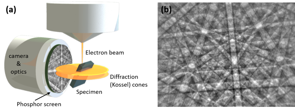
Figure 1: (a) Illustration of the EBSD detection geometry and a conventional EBSD detector. (b) EBSP from a GaN think film at an electron beam energy of 20 keV.
An electron backscatter diffraction pattern (EBSP) from a GaN thin film is shown in Figure 1(b). A detailed description of the intensities in EBSPs is possible using a Bloch wave approach to the dynamical theory of electron diffraction [13, 14]; however, the geometry of the EBSP can be described, to a first approximation, by considering the angular position of electrons which have been Bragg reflected from the lattice planes of the crystal specimen. On penetrating the specimen, the electrons of the impinging beam are both elastically and inelastically scattered. This creates a diverging source of electrons with a broad range of energies [2, 15, 16, 17, 18, 19, 20, 21]. The elastically scattered electrons and quasi-elastically scattered electrons (those electrons which have lost only a relatively small amount of energy through phonon or plasmon scattering) may travel in such a way that their energy and direction satisfy the Bragg condition, 2dsinθ=nλ, for a set of planes and undergo diffraction, where d is the spacing between planes, θ is the Bragg angle, λ the wavelength of the electron and n the order of diffraction. Because of the cylindrical symmetry of the Bragg reflection condition with respect to the lattice plane normal, diffraction cones (Kossel cones) are formed. When these cones intersect the phosphor screen, Kikuchi lines are observed in a gnomonic projection: see Figure 1(a). The Kikuchi lines appear as almost straight lines because the cones are very shallow, as the Bragg angle θ is of order 1°. The Kikuchi lines are superimposed on a diffuse background which is produced predominantly by lower energy inelastically scattered electrons which have not been Bragg scattered. As each Kikuchi band (pair of Kikuchi lines) is effectively fixed to the plane from which it is formed, an EBSD pattern provides a direct measurement of a sample’s orientation. Rotation of a crystal will produce a rotation of the EBSP; a tilt of a crystal will produce a shift in the EBSP; and and strain/distortion of the the crystal will distor the EBSP (see Figure 2).
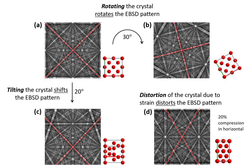
Figure 2: Effect of rotation, tilt and strain on the EBSP of a single crystal silicon: (a) Si (100), (b) crystal rotated by 30°, (c) crystal tilted by 20° and (d) 20% compression along the x-axis (horizontal). The inset placed on the right side of each pattern shows the corresponding real space views of the crystal structure.
An EBSP contains a large amount of crystallographic information from which it is possible to deduce the phase of the material under study. The space group may be determined by analysing the symmetry exhibited by the pattern. An unknown phase may be identified by a comparison of the observed symmetry with the symmetry of a list of known phases contained in a database until it is correctly identified [22].
References